Asynchronous Circuit and System Design Group
Asynchronous Open-Source DLX Processor (ASPIDA)
| Desynchronization: an easy approach to Asynchronous design |
- J. Cortadella, A. Kondratyev, L. Lavagno and C. Sotiriou. A Concurrent Model for De-synchronization. In Handouts of the International Workshop on Logic Synthesis, pages 294-301, 2003. (pdf)
- I. Blunno, J. Cortadella, A. Kondratyev, K. Lwin and C. Sotiriou. Handshake Protocols for De-synchronization. In Proceedings of the 10th International Synposium on Asynchronous Circuits and Systems, April 2004. (pdf)
Overview
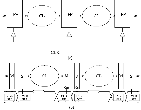
The de-synchronization approach presented in this section aims at the substitution of the global clock of a circuit by a set of asynchronous controllers that guarantee an equivalent behavior. The method assumes that the circuit has combinational blocks (CL) and registers implemented with D flip-flops (FF), all of them working with the same clock edge (e.g. rising in Figure 1(a)).
The de-synchronization method proceeds in three steps:
- Conversion of the flip-flop-based synchronous circuit into a
latch-based one
(
 and
and  latches in Figure 1(b)) by:
decoupling local clocks for master and slave latches and
(optionally)
improving performance through retiming, i.e. by moving latches
across
combinational logic.
- Generation of matched delays for combinational logic (denoted by rounded rectangles in Figure 1(b)). Each matched delay must be greater than the delay of the critical path of the corresponding combinational block.
- Interconnection of controllers for local clocks.
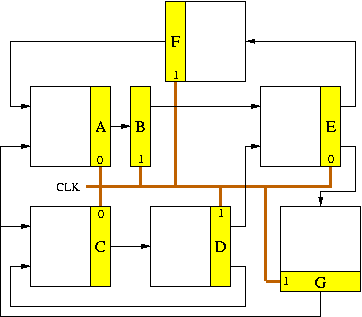
Figure 2 depicts a
synchronous netlist after conversion
into latch-based design, possibly after applying
the retiming mentioned above. The shadowed boxes
represent latches, whereas the white boxes represent combinational
logic. Latches must alternate their phases. Latches with a label
![]() (
(![]() ) at the clock input represent the even
(odd) latches, transparent when the clock is low (high).
Data transfers must always occur from even (master)
to odd (slave) latches and vice-versa.
) at the clock input represent the even
(odd) latches, transparent when the clock is low (high).
Data transfers must always occur from even (master)
to odd (slave) latches and vice-versa.
Initially, only the latches corresponding to one of the phases store valid data. Without loss of generality, we will assume that these are the even latches. The odd latches store bubbles, in the argot of asynchronous circuits.
Marked Graphs
Marked Graphs (MG) is the formalism used in this document to model de-synchronization. They are a subclass of Petri nets that can model decision-free concurrent systems [10].
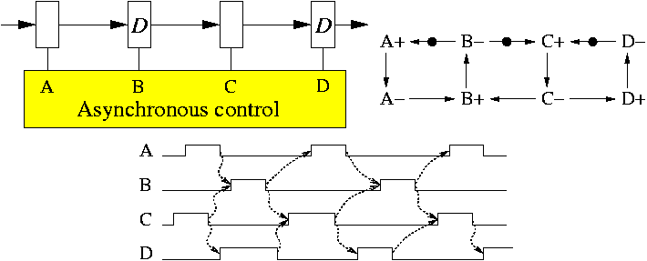
An example of marked graph is shown in Figure 3, where the events ![]() and
and ![]() represent the rising and falling transitions of signal
represent the rising and falling transitions of signal ![]() ,
respectively. Under the given initial marking (denoted by solid dots
at arcs) two events are enabled
,
respectively. Under the given initial marking (denoted by solid dots
at arcs) two events are enabled ![]() and
and ![]() . The sequence of events
. The sequence of events
![]() is an example of a feasible sequence of the
marked graph.
is an example of a feasible sequence of the
marked graph.
Liveness and safeness are properties of marked graphs relevant for our work. Liveness ensures that any event can be fired infinitely often from any reachable marking. Safeness ensures that no arc will have more than one token in any reachable marking. The following result was proven in [2].
De-synchronization models
This section presents two models for de-synchronization. The first one is presented for its simplicity, and can be considered as a restricted case of the second.
For the sake of simplicity, we will also assume that all combinational blocks and latches have zero delay. Thus, the only important thing about the model is the sequence of events of the latch control signals. A timed model, and its performance, will be presented in Section 4.
Non-overlapping de-synchronization model. In the synchronous methodology, latched designs are normally clocked by two-phase non-overlapping clocks. The first model is a direct implementation of this scheme.
A timing diagram and the corresponding marked
graph for a simple pipeline is
depicted in Fig. 3.
The latches are transparent when the control signal is
high. Initially, only half of the
latches contain data (![]() ). Data items flow in such
a way that
a latch never captures a new item before the successor latch has
captured the previous one.
). Data items flow in such
a way that
a latch never captures a new item before the successor latch has
captured the previous one.
Since the pulses for adjacent latches are non-overlapping, data overwriting can never occur. However, contrary to common belief, the need for a non-overlapping scheme to avoid races could be relaxed, as discussed below.
Overlapping de-synchronization model.
Figure 4 shows
another model that allows clock pulses of
adjacent latches to overlap. This model is based on the
observation
that a data item can ripple through more than one latch, as long as the
previous values stored in those rippling latches have already been
captured
by the successor latches. As an example, event ![]() can
fire as
soon as data is available in
can
fire as
soon as data is available in ![]() (arc
(arc ![]() ) and the
previous data in
) and the
previous data in ![]() has been captured by
has been captured by ![]() (arc
(arc ![]() ).
).
The formal model for this de-synchronization is depicted in the marked
graph of Fig 4.
The arc ![]() is
included to model
the alternation of
is
included to model
the alternation of ![]() and
and ![]() at one end of the
pipeline.
This arc is redundant for the other events.
at one end of the
pipeline.
This arc is redundant for the other events.
It is easy to understand that the model of Fig. 3 can be obtained by reducing the concurrency of the model in Fig. 4.
General de-synchronization model. By taking as an example the overlapping model, we now show that it can be used for any arbitrary synchronous netlist, while preserving a property that makes the de-synchronized circuits observationally equivalent to their synchronous versions: flow equivalence [5].
The method for de-synchronizing an arbitrary netlist relies on composition of the controllers. We just identify pairwise interactions between adjacent latches, and then the overall clock generation circuit is obtained through composition of MGs corresponding to these partial descriptions. This procedure creates a marked graph of a certain class that we will call circuit marked graph (CMG).
The specification of a pairwise interaction between even-odd and
odd-even latches for overlapping de-synchronization is shown in
Figure 5. It
models the communication of data from latch ![]() to latch
to latch ![]() . These
patterns exactly correspond to the ones used in the behavioral
specification of a linear pipeline in
Figure 4. The
only difference is that we added two
auxiliary arcs
. These
patterns exactly correspond to the ones used in the behavioral
specification of a linear pipeline in
Figure 4. The
only difference is that we added two
auxiliary arcs ![]() and
and ![]() to model the behavior of the abstracted
parts of the system (those
that precede
to model the behavior of the abstracted
parts of the system (those
that precede ![]() and succeed
and succeed ![]() ).
).
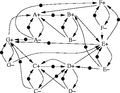
Figure 6 depicts the de-synchronization MG for the circuit in Figure 2, as obtained by composition of patterns from Figure 5.
Properties of the general model
We now discuss several properties of the model. The proofs of the theorems are presented in [3].
Safeness guarantees that no data overwriting will occur.
Liveness guarantees something crucial for the model: absence of
deadlocks. At this point, it is important to emphasize that the
controller for
de-synchronized clocks presented in this document has self-resetting
pulses, i.e. the only causality arc that precedes an event ![]() is the
corresponding
is the
corresponding ![]() . This spontaneous ``return-to-zero''
guarantees liveness for any netlist, even cyclic ones.
We will discuss in Section 6 how to modify matched
delays after layout, so that clock pulses can be delivered reliably
to the latches.
. This spontaneous ``return-to-zero''
guarantees liveness for any netlist, even cyclic ones.
We will discuss in Section 6 how to modify matched
delays after layout, so that clock pulses can be delivered reliably
to the latches.
Flow equivalence
The de-synchronization model previously presented enables data to flow across an asynchronous circuit. But is this data flow equivalent to the behavior of the synchronous circuit?
We now present the notion of flow-equivalence [5], which is related to that of synchronous behavior in [9], in terms of the projection of traces onto the latches of the circuit.
Intuitively, two circuits are flow-equivalent if their behavior cannot be distinguished by observing the sequence of values stored at each latch. This observation is done individually for each latch and, thus, the relative order at which values are stored in different latches can change.
Timed model
The model presented in Section 3 guarantees synchronous equivalence with zero-delay components. However, computational blocks and latches have delays that impose a set of timing constraints for the model to be valid.
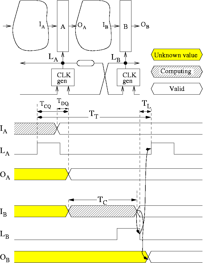
Figure 7
depicts the timing diagram for the behavior of
two latches in a pipeline. The signals ![]() and
and ![]() represent the
inputs and outputs of the latches. The signal
represent the
inputs and outputs of the latches. The signal ![]() is
the control of
the latch (
is
the control of
the latch (![]() for transparent).
for transparent).
We will focus our attention on latch ![]() . As soon as
. As soon as ![]() becomes
valid, the computation for block
becomes
valid, the computation for block ![]() starts. Latch
starts. Latch ![]() can become
transparent before the computation completes. Opening a latch in
advance is beneficial
for performance, because it eliminates the time for capturing data from
the
critical path.
can become
transparent before the computation completes. Opening a latch in
advance is beneficial
for performance, because it eliminates the time for capturing data from
the
critical path.
Once the computation is over, the local clock ![]() of
the destination
latch
of
the destination
latch ![]() immediately falls. This is possible because
modern latches
have zero setup time [1].
immediately falls. This is possible because
modern latches
have zero setup time [1].
Assuming that all controllers have similar delays the following
constraint is required for correct
operation.
The constraint (1)
indicates that the cycle time of a local
clock (measured as a delay ![]() between two
rising edges of
between two
rising edges of ![]() ), must be greater than the delay of local
clock propagation though a latch (
), must be greater than the delay of local
clock propagation though a latch (![]() ) plus the
delay of the
computational block (
) plus the
delay of the
computational block (![]() )
plus the latch controller delay (
)
plus the latch controller delay (![]() ). The control
overhead in
this scheme is reduced to a single delay
). The control
overhead in
this scheme is reduced to a single delay ![]() because control
handshake overlaps with the computation cycle due to the early rising
of the local clock. The constraint assumes
that the depth of combinational logic is sufficiently large to
amortize the overlapping part of the handshake. The latter is true for
ASIC designs, that often have more than 20 levels of logic between
adjacent registers. However, we also tried examples, such as
a DES encryption engine,
which are extremely shallow, with similar results.
because control
handshake overlaps with the computation cycle due to the early rising
of the local clock. The constraint assumes
that the depth of combinational logic is sufficiently large to
amortize the overlapping part of the handshake. The latter is true for
ASIC designs, that often have more than 20 levels of logic between
adjacent registers. However, we also tried examples, such as
a DES encryption engine,
which are extremely shallow, with similar results.
Inequality (1) guarantees the satisfaction of set-up constraints for the latch. Note that hold constraints in a de-synchronized circuit are ensured automatically, because the clock of any predecessor latch rises only after the clock of its successor latch had fallen. This makes it impossible to have races between two consecutive data items at latch inputs.
Timing compatibility
To prove that the suggested design methodology is modular and compositional we need to show that a de-synchronized circuit can replace its synchronous counterpart without disturbing the rest of a system (presumably synchronous). This can be achieved by comparing cycle times of de-synchronized and synchronous designs.
In a synchronous flip-flop-based circuit, the cycle time ![]() is
bounded by [1]:
is
bounded by [1]:
There is a small caveat in the above statement. The notion of a cycle time is well defined only for a circuit with a periodic clock. In a de-synchronized system the separation time between adjacent rising edges of the same local clock might change during functioning. Therefore when talking about de-synchronized and synchronous systems one has to relate the perfect periodic behavior of one of them to a non-periodic one of another.
Two facts proven in [3] help in establishing this relationship.
- Latches that belong to critical computational paths of a
de-synchronized system have a well-defined constant cycle time
 .
.
- The rest of the latches might have variable cycle times in the
finite prefix of a system functioning but finally must settle to
constant cycle time
 .
.
This shows that the behavior of a de-synchronized circuit has a well-defined periodicity, similar to that of a synchronous one, paced by a common clock.
A de-synchronized circuit with cycle time ![]() can
be embedded
into a synchronous environment
with a clock cycle
can
be embedded
into a synchronous environment
with a clock cycle ![]() by driving the latch
controllers on its boundaries
with the clock (as if it was coming from ``external'' controllers).
This does
not cause any meta-stability problems and satisfies setup and hold
constraints,
as long as
by driving the latch
controllers on its boundaries
with the clock (as if it was coming from ``external'' controllers).
This does
not cause any meta-stability problems and satisfies setup and hold
constraints,
as long as ![]() . Under these conditions,
boundary
latches become critical, since
they are paced by external clock
. Under these conditions,
boundary
latches become critical, since
they are paced by external clock ![]() . This makes
de-synchronized
and synchronous systems compatible in terms of timing,
because their external timed behavior is the same.
. This makes
de-synchronized
and synchronous systems compatible in terms of timing,
because their external timed behavior is the same.
One advantage of de-synchronization is that it eases some form of circuit binning based on performance. If we assume that the performance of similar objects (e.g. transistors, interconnects on the same layer) track each other within relatively small regions of the layout, we can assume that the performance of a die will be determined by the delay chains, while the delay of the logic will be proportionately smaller, and thus setup constraints will be automatically satisfied.
This means that the request and acknowledge wires at the boundaries of the circuit can be used to measure the worst-case response time of every individual die. In other terms, the maximum speed of a die can be established by only looking at the timing of transitions of some output signals with respect to the clock input, without the need for expensive at-speed delay testing equipment. This allows one to classify dies according to their maximum operational speed (binning), which so far was only used for leading-edge CPUs (from Intel, AMD, Sun) due to the huge cost of at-speed testing equipment. It also allows one to tune the process, by observing the performance of whole circuits, not just of small delay chains on test chips.
Implementation of the model
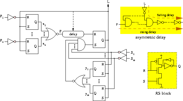
Figure 8
depicts a possible implementation of
the controller. Inputs ![]() ...
...![]() are the
are the ![]() signals of its
signals of its ![]() predecessor
controllers, while inputs
predecessor
controllers, while inputs ![]() ...
...![]() are the
are the ![]() signals of its
signals of its ![]() successor controllers.
considered. The delay element must have a delay for the
rising transition which is
larger than that of the combinational
block, while the falling transition delay determines the pulse width.
Such an asymmetric delay chain can be built easily with not
and nand gates.
successor controllers.
considered. The delay element must have a delay for the
rising transition which is
larger than that of the combinational
block, while the falling transition delay determines the pulse width.
Such an asymmetric delay chain can be built easily with not
and nand gates.
The sequence of events that determines the corresponding
delays is the following:

This is not the only way to implement these controllers. The semi- and fully-decoupled controllers presented in [4] are also valid, although a formal proof of their correctness in this context is more complicated. Similarly for the controllers presented in [12,13,14].
Physical Design and Testing
Matched Delay Insertion. The flow that we used for the
de-synchronization approach
begins with a synthesizable HDL specification
(e.g. Verilog/VHDL), using the conventional synchronous HDL
constructs. Next, each datapath
element is synthesized for the target cycle time ![]() ,
using a conventional synthesis tool.
Due to the load of the local clock by the registers of
the datapath block, buffers are inserted at this stage.
,
using a conventional synthesis tool.
Due to the load of the local clock by the registers of
the datapath block, buffers are inserted at this stage.
The circuit is analyzed using conventional static timing analysis tools to estimate the delay of each matched delay element. These matched delay elements are generated and embedded into latch controllers. At this stage, the datapath blocks and their corresponding latch controllers are combined to form the complete netlist of the de-synchronized circuit. Once the complete netlist is assembled, it may be simulated and its correct operation verified using a gate-level simulator.
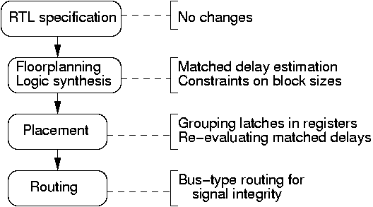
The circuit is then placed and routed, and the post-layout delays are extracted. The pessimistic delays used for pre-layout timing analysis are now more precise, and redundant not and nand gate pairs can be removed from the delay chains, by exploiting the incremental place-and-route capabilities of modern tools. The possible modifications of different stages in conventional automatic design flow for doing de-synchronization are shown in Figure 9.
Design for Testability.
The datapath can be tested by using scan path insertion
with synchronous tools. A clock can be distributed to every register
and used only in test mode. Local
acknowledge wires in test mode allow one to build this network without
skew
problems. Thus it is considerably smaller than in the
synchronous case, where it must satisfy tight skew constraints.
Moreover, it is kept idle during normal operation.
Asynchronous handshake circuits can also be tested by using a full-scan methodology, as discussed in [11]. This has a performance and area overhead, but it is essential for the acceptance of the methodology. The goal is to ensure full coverage. Handshake circuits are self-checking, and the work in [7] showed that 100% stuck-at coverage can be achieved for asynchronous pipelines using conventional test pattern generation tools.
De-Synchronization Case Study
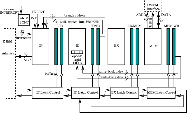
We present results on the application of
de-synchronization to a DLX processor.
The de-synchronized DLX consists of five architectural DLX pipeline
stages, four of which
actually correspond to circuit blocks (at the circuit level WB is
merged with
ID). Each block is controlled by its own latch controller. The arrows
of the latch controllers correspond to their ![]() and
and ![]() signals,
and illustrate the datapath dependencies. Stages ID, EX and MEM form a
ring. ID
is the heart of the processor containing the Register File and all
hazard-detection logic and synchronizes stages IF and MEM. Thus,
instructions
leaving MEM (for WB) will synchronize with instructions coming from IF.
This is
indeed necessary for handling data dependencies, as a register being
written
may be the same with the one needing to be read in a current
instruction.
Data hazard detection takes place by ID comparing the output register
of
instructions in other pipeline stages and their opcodes, and deciding
on
inserting the correct number of NOPs.
signals,
and illustrate the datapath dependencies. Stages ID, EX and MEM form a
ring. ID
is the heart of the processor containing the Register File and all
hazard-detection logic and synchronizes stages IF and MEM. Thus,
instructions
leaving MEM (for WB) will synchronize with instructions coming from IF.
This is
indeed necessary for handling data dependencies, as a register being
written
may be the same with the one needing to be read in a current
instruction.
Data hazard detection takes place by ID comparing the output register
of
instructions in other pipeline stages and their opcodes, and deciding
on
inserting the correct number of NOPs.
After the initial synthesis of each circuit block using latches, the whole design is optimized incrementally to meet all timing requirements. Max-delay constraints between latches are used to ensure cycle time in the datapaths but the control blocks are untouched inside G2C-RC, our synthesis tool. Then the gate-level netlist and matching timing constraints are imported into SoC Encounter. Floor-planning is done along with creation of power structures inside Encounter. All the standard cells are placed using Amoeba and routed with NanoRoute. Post-route optimization is iterated until all timing violations are fixed. The synchronous DLX is obtained using the same flow with the additional step of Clock Tree Synthesis in Encounter before the Route stage.
Table 1 contrasts the characteristics of the synchronous and of the de-synchronized DLX. The data are post-layout results based on gate-level simulations with back-annotation of extracted parasitics.
|
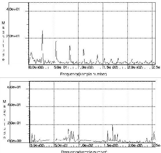
One can see that both designs have approximately the same area, speed and power consumption. The Electro-Magnetic Emission cannot be effectively measured without fabricating the chip. However, we estimate the advantages of de-synchronization in this respect by measuring, with a power analysis tool, the waveform of the current absorbed by the circuit from the power rails. Its spectrum, shown in Figure 11 for the synchronous FF-based circuit and the de-synchronized one (the synchronous latch-based one had similar characteristics) shows approximately 30% lower emission peaks in the desynchronized case, which should also be reflected in lower EMI.
Unfortunately about half of the circuit gates and flip-flops (due to the register file) is contained in the ID stage, which has a very complex local clock tree. This represents a worst-case for our methodology, since the ID stage is almost as noisy as the original synchronous circuit, but we are still able to show advantages with respect to a purely synchronous implementation in terms of estimated Electro-Magnetic Emission.
Bibliography
-
- 1
- D. Chinnery and K. Keutzer.
Reducing the timing overhead.
In Closing the Gap between ASIC and Custom: Tools and Techniques for High-Performance ASIC design, chapter 3. Kluwer Academic Publishers, 2002. - 2
- F. Commoner, A. W. Holt, S. Even, and
A. Pnueli.
Marked directed graphs.
Journal of Computer and System Sciences, 5:511-523, 1971. - 3
- J. Cortadella, A. Kondratyev, L. Lavagno, and
C. Sotiriou.
A concurrent model for de-synchronization.
Extended version of paper presented at IWLS03. http://www.lsi.upc.es/~jordicf/publications/pdf/iwls03_extended.pdf. - 4
- S. B. Furber and P. Day.
Four-phase micropipeline latch control circuits.
IEEE Transactions on VLSI Systems, 4(2):247-253, June 1996. - 5
- P. L. Guernic, J.-P. Talpin, and J.-C. L. Lann.
Polychrony for system design.
Journal of Circuits, Systems and Computers, Apr. 2003. - 6
- R. Kol and R. Ginosar.
A doubly-latched asynchronous pipeline.
In Proc. International Conf. Computer Design (ICCD), pages 706-711, Oct. 1996. - 7
- A. Kondratyev, L. Sorenson, and A. Streich.
Testing of asynchronous designs by inappropriate means: Synchronous approach.
In Proc. IEEE Int. Symp. on Advanced Research in Asynchronous Circuits and Systems. IEEE Computer Society Press, March 2001. - 8
- M. Ligthart, K. Fant, R. Smith, A. Taubin,
and A. Kondratyev.
Asynchronous design using commercial HDL synthesis tools.
In Proc. International Symposium on Advanced Research in Asynchronous Circuits and Systems, pages 114-125. IEEE Computer Society Press, Apr. 2000. - 9
- D. H. Linder and J. C. Harden.
Phased logic: Supporting the synchronous design paradigm with delay-insensitive circuitry.
IEEE Transactions on Computers, 45(9):1031-1044, Sept. 1996. - 10
- T. Murata.
Petri Nets: Properties, analysis and applications.
Proceedings of the IEEE, pages 541-580, Apr. 1989. - 11
- O. A. Petlin and S. B. Furber.
Scan testing of micropipelines.
In Proc. IEEE VLSI Test Symposium, pages 296-301, May 1995. - 12
- S. Schuster, W. Reohr, P. Cook, D. Heidel,
M. Immediato, and K. Jenkins.
Asynchronous Interlocked Pipelined CMOS Circuits Operating at GHz.
GHz.
In International Solid State Circuits Conference, pages 292-293, Feb. 2000. - 13
- M. Singh and S. M. Nowick.
MOUSETRAP: Ultra-high-speed transition-signaling asynchronous pipelines.
In Proc. International Conf. Computer Design (ICCD), pages 9-17, Nov. 2001. - 14
- I. Sutherland and S. Fairbanks.
GasP: A minimal FIFO control.
In Proc. International Symposium on Advanced Research in Asynchronous Circuits and Systems, pages 46-53. IEEE Computer Society Press, Mar. 2001. - 15
- M. A. Thornton, K. Fazel, R. B. Reese, and
C. Traver.
Generalized early evaluation in self-timed circuits.
In Proc. Design, Automation and Test in Europe (DATE), pages 255-259, Mar. 2002. - 16
- V. Varshavsky, V. Marakhovsky, and T.-A. Chu.
Logical timing (global synchronization of asynchronous arrays.
In The First International Symposium on Parallel Algorithm/Architecture Synthesis, pages 130-138, Aizu-Wakamatsu, Japan, Mar. 1995.
2004-04-03
