|
Asynchronous Circuit and System Design Group
|
Asynchronous Open-Source DLX Processor (ASPIDA)
|
Synthesis Procedure Summary
|
| |

General information
This page summarizes the options that we used for the synthesis of the
asynchronous DLX. The target device is a Spartan IIE and more
specifically the xcs2s200e
device. We restricted the maximum fanout of the nets to 100 and allowed
register duplication. The optimization effort targets area and the
design is flattened, which means that we do not preserve the hierarchy
of the design.
Asynchronous DLX
The approach of the implementation of a de-synchronized circuit is
different
than the approach used in a synchronous circuit. The absence of a clock
and the presence of special asynchronous elements in the circuit
introduces a number of difficulties that need to be dealt with.
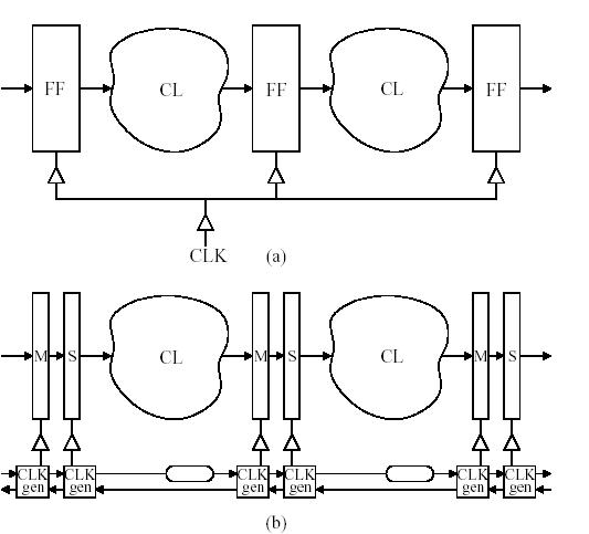
Delay elements are necessary in a de-synchronized circuit in order to
match the delay of combinational logic present between a pair of
latches. In the timed de-synchronization model a latch should only be
enabled after data have arrived at its inputs, thus delay elements
matching the delay of combinational logic blocks are used to enforce
correct timing, as shown in the figure below.

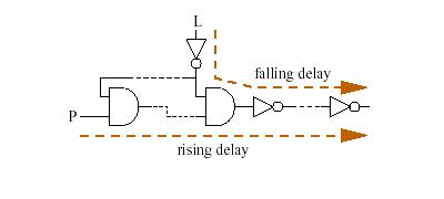
As data propagate only during the valid phase of the handshake between
controllers and not during the return-to-zero phase, assymetric delay
elements are used. The figure below shows a possible implementation of
an assymetric delay element.

DLX Controllers
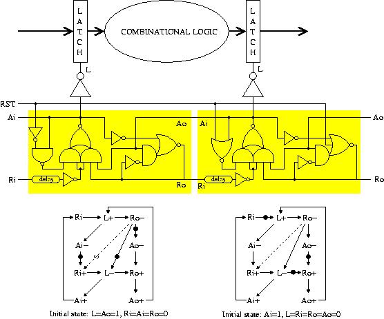
Figure below shows the implementation of
the DLX controllers. The controllers below coresponds to an
implementation of the semi-decoupled four-phase handshake protocol.
Figure below depicts an implementation,
with static CMOS gates, of a pair of controllers (even and odd) for a
fragment of data-path. The figure also shows the marked graphs modeling
the behavior of each controller. The only difference is the initial
marking, that determines the reset logic (signal RST).

Resetting the
controllers is crucial for a correct behavior. In this case, the even
latches are transparent and the odd latches opaque in the initial
state. With this strategy, only the odd latches must be reset in the
data-path. The implementation also assumes a relative timing constraint
(arc Ro- ---> Ri+) that can be easily met with the actual design.
The controllers also include a delay that must be
matched with the delay of the combinational logic incremented by the
pulse width
of the latch control signal. The implementation of the symmetric
(pulse) and the asymmetric
(matched) delay elements of the controllers for the DLX is shown in the
figure below. The pulse delay consist of a chain of an even number of
inverters, and the matched delay of a chain of AND gates, where the
longest path of the matched delay is equal to the corresponding delay
of the critical path of the combinational logic.
DLX Synthesis
Our asynchronous DLX has five pipeline stages, which are separated by
flip-flops. Asynchronous controllers provide the flip-flops with the
appropriate signals so that the data move safely from one pipeline
stage to the other. In order for these signals to arrive at the
flip-flops at approximately the same moment, we used low skew lines.
However, this approach proved to be insufficient for the Instruction
Decode and the Execute stage, which happen to be the two stages with
the most combinatorial logic. The signals from the controllers had to
be reinforced by buffers.
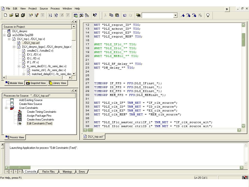
The datapath optimization was performed by optimizing each pipeline
stage independently. Two timing groups have been created for each pair
of
stages of the pipeline. The first group contains all the flip-flops of
the
pipeline stage that the signals to be analyzed begin from. The second
group
contains all the flip-flops of the next pipeline stage. After applying
``FROM-TO''
constraints to the generated groups, a timing analysis is performed to
the
path that the groups form. The results of the static timing analysis
represent
the delay of the datapath. This delay shows the minimum delay that the
delay elements must have in order for the circuit to operate correctly.
It is necessary to emphasize that the delay elements were excluded from
the optimization of the datapath for two reasons. The first reason is
that the delay elements do not belong to the datapath and the second
reason is that we are not interested in minimizing the delay of a delay
element, but rather bounding it within predefined limits. The synthesis
directive for the exclusion of the delay elements from the timing
optimization is the ``TIG'' constraint (a.k.a. Timing IGnore).
VGA Controller
The clock of the VGA controller has half the frequency of the clock
that the board provides. The board has a clock of 20ns (50 MHz) and the
VGA controller needs a clock of 40ns (25MHz). In order to create the
appropriate frequency for the VGA controller, we used a clock divider
that has as input the clock that the board provides and outputs the
clock for the VGA controller. The clock divider is configured to divide
the clock frequency by a factor of 2. For more information on the use
of clock dividers in Xilinx devices, refer to the Xilinx
software manuals.
The clock signal of the VGA controller has been configured as a low
skew line. No other synthesis attributes have been applied to the VGA
controller.
|
|