| |
Asynchronous Circuit and System Design Group | ||
Asynchronous Open-Source DLX Processor (ASPIDA)
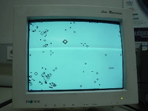
 In the image above you can see the
output of the VGA driver to the display. Clicking on the image will
show it on a larger size.
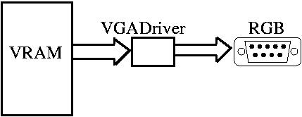
The VGA driver communicates with the video ram where the CPU has stored the data to be displayed.The CPU changes the data in the video ram on a constant basis and the VGA driver reads the latest update of the video ram. There is no direct communication between the VGA driver and the CPU. Figure below illustrates the interfaces of the VGA driver.  The clock of the VGA controller has half the frequency of the clock that the board provides. The board has a clock of 20ns (50 MHz) and the VGA controller needs a clock of 40ns (25 MHz). In order to create the appropriate frequency for the VGA controller, we used a clock divider that has as input the clock that the board provides and outputs the clock for the VGA controller. The clock divider is configured to divide the clock frequency bu a factor of 2. The clock signal of the VGA controller has been configured as a low skew line. |
|||