Asynchronous Open-Source DLX Processor (ASPIDA)
Computational blocks
and latches have delays that impose a set of timing constraints for
the model to be valid.
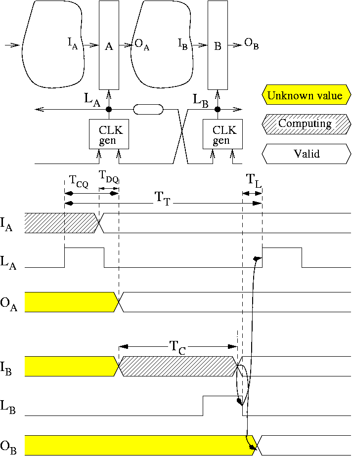
Figure 1
depicts the timing diagram for the behavior of
two latches in a pipeline. The signals I and O represent the
inputs and outputs of the latches. The signal L is the control of
the latch (L=1 for
transparent).
We will focus our attention on latch A. As soon as OA
becomes
valid, the computation for block B
starts. Latch B can become
transparent before the computation completes. Opening a latch in
advance is beneficial
for performance, because it eliminates the time for capturing data from
the
critical path.
Once the computation is over, the local clock LB
of the destination
latch B immediately falls.
This is possible because modern latches
have zero setup time [1].
Figure 1:
Timing constraints for the asynchronous controllers.
 |
Assuming that all controllers have similar delays the following
constraint is required for correct
operation.
The constraint (1)
indicates that the cycle time of a local
clock (measured as a delay TT
between two
rising edges of LA),
must be greater than the delay of local clock
propagation though a latch (TCQ)
plus the delay of the
computational block (TC)
plus the latch controller delay (TL).
The control overhead in
this scheme is reduced to a single delay TL
because control
handshake overlaps with the computation cycle due to the early rising
of the local clock. The constraint assumes
that the depth of combinational logic is sufficiently large to
amortize the overlapping part of the handshake. The latter is true for
ASIC designs, that often have more than 20 levels of logic between
adjacent registers. However, we also tried examples, such as
a DES encryption engine,
which are extremely shallow, with similar results.
Inequality (1)
guarantees the satisfaction of set-up constraints for the latch. Note
that hold constraints in a
de-synchronized circuit are ensured automatically, because the clock of
any predecessor latch rises only after the clock of its successor
latch had fallen. This makes it impossible to have races between two
consecutive
data items at latch inputs.
Timing compatibility
To prove that the suggested design methodology is modular and
compositional we need to show that a de-synchronized circuit can
replace its synchronous counterpart without disturbing the rest of a
system (presumably synchronous). This can be achieved by comparing
cycle times of de-synchronized and synchronous designs.
In a synchronous flip-flop-based circuit, the cycle time TS is
bounded by [1]:
| TS >= TC
+ Tsetup + Tskew
+ TCQ |
(2) |
where TC, Tsetup,
Tskew and TCQ
are maximum
combinational logic, setup, skew and
clock-to-output times respectively.
Let us compare inequalities (1)
and (2),
bearing in
mind that due to retiming the maximal computation time in a
de-synchronized
circuit can only be reduced. We can conclude that under
reasonable timing assumption ( Tsetup
+ Tskew >= TL)
the cycle time of
de-synchronized
circuit TT
should not be larger than the cycle time TS of
the corresponding
synchronous design.
There is a small caveat in the above statement. The notion of a
cycle
time is well defined only for a circuit with a periodic clock. In a
de-synchronized system the separation time between adjacent rising
edges of the
same local
clock might change during functioning.
Therefore when talking about de-synchronized and synchronous
systems one has to relate the perfect periodic behavior of one of them
to
a non-periodic one of another.
Two facts proven in [3]
help in establishing this relationship.
- Latches that belong to critical computational paths of a
de-synchronized system have a well-defined constant cycle time TT.
- The rest of the latches might have variable cycle times in
the finite prefix of a system functioning but finally must settle to
constant cycle time TT.
This shows that the
behavior of a de-synchronized circuit has a well-defined periodicity,
similar to that of a synchronous one, paced by a common clock.
A de-synchronized circuit with cycle time TT can be embedded
into a synchronous environment
with a clock cycle TS
by driving the latch controllers on its boundaries
with the clock (as if it was coming from ``external'' controllers).
This does
not cause any meta-stability problems and satisfies setup and hold
constraints,
as long as TS
>= TT. Under these conditions,
boundary
latches become critical, since
they are paced by external clock TS.
This makes de-synchronized
and synchronous systems compatible in terms of timing,
because their external timed behavior is the same.
One advantage of de-synchronization is that it eases some
form of circuit binning based on performance. If we assume
that the performance of similar objects (e.g. transistors,
interconnects on the same layer) track each other within relatively
small regions of the layout, we can assume that the performance
of a die will be determined by the delay chains, while the delay
of
the logic will be proportionately smaller, and thus setup constraints
will be automatically satisfied.
This means that the request and acknowledge wires at the boundaries
of
the circuit can be used to measure the worst-case response time of every
individual die. In other terms, the maximum speed of a die can be
established by only looking at the timing of transitions of some output
signals
with respect to the clock input, without the need for expensive
at-speed delay
testing equipment. This allows one to classify dies according to their
maximum operational speed (binning), which so far was only used for
leading-edge CPUs (from Intel, AMD, Sun) due to the huge cost of
at-speed
testing equipment. It also allows one to tune the process, by observing
the performance of whole circuits, not just of small delay chains on
test chips.
|
