Asynchronous Circuit and System Design Group
Asynchronous Open-Source DLX Processor (ASPIDA)
| Implementation of the model |
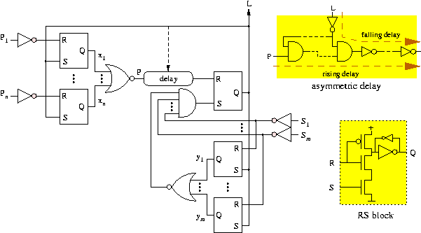
Figure 1 depicts a possible implementation of the controller. Inputs P1 ...Pn are the L signals of its n predecessor controllers, while inputs S1 ...Sm are the L signals of its m successor controllers. considered. The delay element must have a delay for the rising transition which is larger than that of the combinational block, while the falling transition delay determines the pulse width. Such an asymmetric delay chain can be built easily with not and nand gates.
The sequence of events that determines the corresponding
delays is the following:

This is not the only way to implement these controllers. The semi- and fully-decoupled controllers presented in [4] are also valid, although a formal proof of their correctness in this context is more complicated. Similarly for the controllers presented in [12,13,14].
Physical Design and Testing
Matched Delay Insertion. The flow that we used for the de-synchronization approach begins with a synthesizable HDL specification (e.g. Verilog/VHDL), using the conventional synchronous HDL constructs. Next, each datapath element is synthesized for the target cycle time TT, using a conventional synthesis tool. Due to the load of the local clock by the registers of the datapath block, buffers are inserted at this stage.
The circuit is analyzed using conventional static timing analysis tools to estimate the delay of each matched delay element. These matched delay elements are generated and embedded into latch controllers. At this stage, the datapath blocks and their corresponding latch controllers are combined to form the complete netlist of the de-synchronized circuit. Once the complete netlist is assembled, it may be simulated and its correct operation verified using a gate-level simulator.
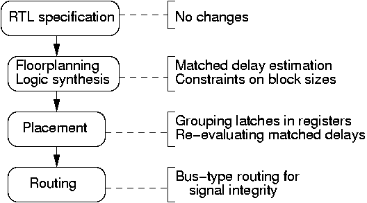
The circuit is then placed and routed, and the post-layout delays are extracted. The pessimistic delays used for pre-layout timing analysis are now more precise, and redundant not and nand gate pairs can be removed from the delay chains, by exploiting the incremental place-and-route capabilities of modern tools. The possible modifications of different stages in conventional automatic design flow for doing de-synchronization are shown in Figure 2.
Design for Testability.
The datapath can be tested by using scan path insertion
with synchronous tools. A clock can be distributed to every register
and used only in test mode. Local
acknowledge wires in test mode allow one to build this network without
skew
problems. Thus it is considerably smaller than in the
synchronous case, where it must satisfy tight skew constraints.
Moreover, it is kept idle during normal operation.
Asynchronous handshake circuits can also be tested by using a full-scan methodology, as discussed in [11]. This has a performance and area overhead, but it is essential for the acceptance of the methodology. The goal is to ensure full coverage. Handshake circuits are self-checking, and the work in [7] showed that 100% stuck-at coverage can be achieved for asynchronous pipelines using conventional test pattern generation tools.
De-Synchronization Case Study
We present results on the application of
de-synchronization to a DLX processor.
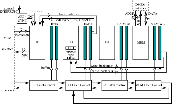
The de-synchronized DLX consists of five architectural DLX pipeline
stages, four of which
actually correspond to circuit blocks (at the circuit level WB is
merged with
ID). Each block is controlled by its own latch controller. The arrows
of the latch controllers correspond to their ![]() and
and ![]() signals,
and illustrate the datapath dependencies. Stages ID, EX and MEM form a
ring. ID
is the heart of the processor containing the Register File and all
hazard-detection logic and synchronizes stages IF and MEM. Thus,
instructions
leaving MEM (for WB) will synchronize with instructions coming from IF.
This is
indeed necessary for handling data dependencies, as a register being
written
may be the same with the one needing to be read in a current
instruction.
Data hazard detection takes place by ID comparing the output register
of
instructions in other pipeline stages and their opcodes, and deciding
on
inserting the correct number of NOPs.
signals,
and illustrate the datapath dependencies. Stages ID, EX and MEM form a
ring. ID
is the heart of the processor containing the Register File and all
hazard-detection logic and synchronizes stages IF and MEM. Thus,
instructions
leaving MEM (for WB) will synchronize with instructions coming from IF.
This is
indeed necessary for handling data dependencies, as a register being
written
may be the same with the one needing to be read in a current
instruction.
Data hazard detection takes place by ID comparing the output register
of
instructions in other pipeline stages and their opcodes, and deciding
on
inserting the correct number of NOPs.
After the initial synthesis of each circuit block using latches, the whole design is optimized incrementally to meet all timing requirements. Max-delay constraints between latches are used to ensure cycle time in the datapaths but the control blocks are untouched inside G2C-RC, our synthesis tool. Then the gate-level netlist and matching timing constraints are imported into SoC Encounter. Floor-planning is done along with creation of power structures inside Encounter. All the standard cells are placed using Amoeba and routed with NanoRoute. Post-route optimization is iterated until all timing violations are fixed. The synchronous DLX is obtained using the same flow with the additional step of Clock Tree Synthesis in Encounter before the Route stage.
Table 1 contrasts the characteristics of the synchronous and of the de-synchronized DLX. The data are post-layout results based on gate-level simulations with back-annotation of extracted parasitics.
|
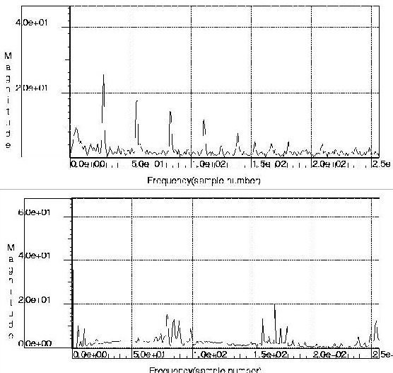
One can see that both designs have approximately the same area, speed and power consumption. The Electro-Magnetic Emission cannot be effectively measured without fabricating the chip. However, we estimate the advantages of de-synchronization in this respect by measuring, with a power analysis tool, the waveform of the current absorbed by the circuit from the power rails. Its spectrum, shown in Figure 3 for the synchronous FF-based circuit and the de-synchronized one (the synchronous latch-based one had similar characteristics) shows approximately 30% lower emission peaks in the desynchronized case, which should also be reflected in lower EMI.
Unfortunately about half of the circuit gates and flip-flops (due to
the
register file) is contained in the ID stage, which has a very complex
local
clock tree. This represents a worst-case for our methodology, since the
ID
stage is almost as noisy as the original synchronous circuit, but we
are still
able to show advantages with respect to a purely synchronous
implementation
in terms of estimated
Electro-Magnetic Emission.


