| |
Asynchronous Circuit and System Design Group | ||
Asynchronous Open-Source DLX Processor (ASPIDA)
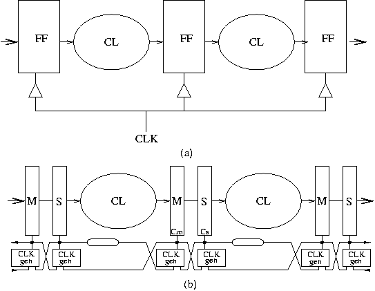
The de-synchronization approach presented in this section aims at the substitution of the global clock of a circuit by a set of asynchronous controllers that guarantee an equivalent behavior. The method assumes that the circuit has combinational blocks (CL) and registers implemented with D flip-flops (FF), all of them working with the same clock edge (e.g. rising in Figure 1(a)). The de-synchronization method proceeds in three steps:
Figure 2 depicts a synchronous netlist after conversion into latch-based design, possibly after applying the retiming mentioned above. The shadowed boxes represent latches, whereas the white boxes represent combinational logic. Latches must alternate their phases. Latches with a label 0 (1) at the clock input represent the even (odd) latches, transparent when the clock is low (high). Data transfers must always occur from even (master) to odd (slave) latches and vice-versa. Initially, only the latches corresponding to one of the phases store valid data. Without loss of generality, we will assume that these are the even latches. The odd latches store bubbles, in the argot of asynchronous circuits. |
|||

